
As hyperscale computing networks continue to evolve at an unprecedented pace, computing interconnects are no longer simply a matter of stacking standardized hardware. Cloud service providers and data center customers are placing increasing emphasis on link-level controllability, refined power management, and long-term total cost of ownership (TCO) optimization.
Against this backdrop, FIBERSTAMP continues to advance its Hybrid semi-DSP technology roadmap. Built around an open optical networking philosophy, the Hybrid approach gives end customers greater control over product usage and a more active role in technology collaboration, enabling differentiated solutions for next-generation high-speed computing interconnects.
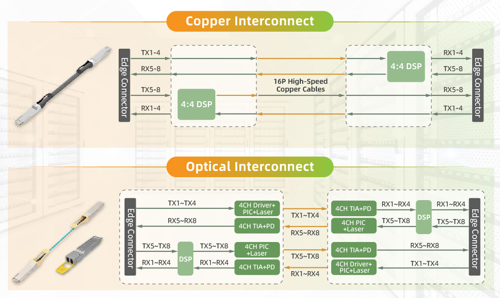
Hybrid Architecture Diagram
An Open and Tunable Alternative to Traditional Full-DSP Architecture
Traditional full-DSP optical modules typically use a closed, fixed-function architecture, with key algorithms and parameters preset by the module vendor.
FIBERSTAMP’s Hybrid architecture retains open parameter-tuning capabilities through the host system. End users can independently configure signal equalization, optical power, and gain strategies without being restricted to fixed algorithm parameters preset by the module vendor.
With this customizable and controllable optical interconnect hardware, customers can build fully autonomous and controllable computing transmission systems. They can optimize performance according to their own traffic patterns and cluster deployment scenarios while maintaining greater control over the underlying network architecture.
DSP-TAP Parameter Tuning via Host System:
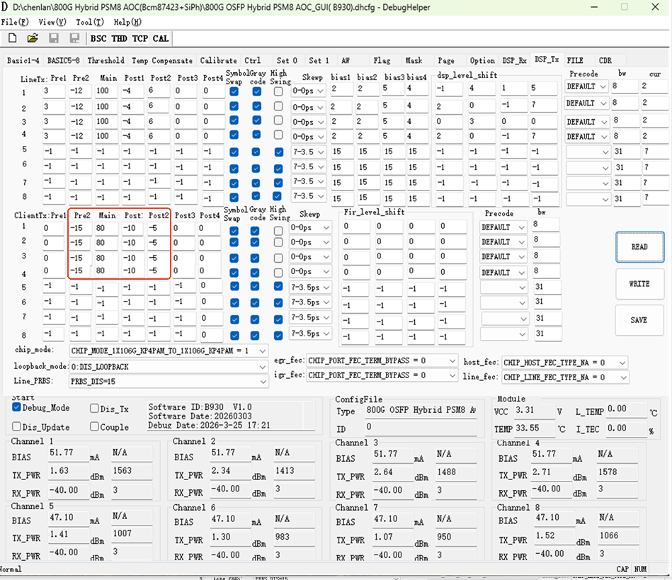
Fine-Grained Parameter Tuning for Power and Cost Optimization
From the customer’s perspective, fine-grained parameter tuning can deliver tangible benefits in both power efficiency and cost control. Across the full lifecycle of AI computing clusters, electricity consumption represents a significant portion of overall operating costs.
With the flexible configuration space provided by FIBERSTAMP’s Hybrid solution, operations teams can reduce module power consumption during periods of low workload while unlocking optimal transmission performance during high-intensity AI training scenarios.
This enables a dynamic balance between performance and power consumption while continuously reducing long-term data center operating costs.
Supporting Joint Validation and Faster Architecture Deployment
Open debugging and tuning capabilities also make it easier for customers to conduct joint validation of self-developed switches and optical engines.
By enabling greater flexibility during system-level testing and optimization, the Hybrid approach can shorten the testing cycle for new architectures and accelerate the deployment and iteration of private computing networks.
Giving Customers a Greater Role in Technology Definition
Beyond the immediate benefits of product usage, the Hybrid model also enables end customers to participate more deeply in technology definition and product evolution.
Traditionally, the technical specifications and performance boundaries of high-speed optical modules have been defined almost entirely by component vendors, leaving customers with limited options beyond selecting from available products.
FIBERSTAMP’s open and tunable Hybrid solution changes this model. Cloud service providers and server OEMs can provide performance optimization requirements based on real-world application scenarios and actively participate in product iteration.
Through closer collaboration between suppliers and customers, both sides can jointly refine interconnect standards optimized for AI computing environments, move beyond commoditized hardware competition, and build a customized high-speed optical interconnect ecosystem designed for next-generation high-performance computing clusters.
Toward More Flexible and Controllable Computing Infrastructure
As global computing infrastructure continues to evolve toward greater diversification and customization, incremental optimization based solely on hardware specification upgrades is increasingly unable to satisfy the deeper requirements of leading computing customers.
FIBERSTAMP remains committed to its differentiated Hybrid technology roadmap. Through an open and tunable product architecture, FIBERSTAMP puts greater control of network optimization back into the hands of customers, empowering them to build energy-efficient, flexible, and fully controllable computing infrastructure.
At the same time, this approach opens a new model of collaborative innovation for the global high-speed optical interconnect industry, enabling closer collaboration between suppliers and customers in the development of next-generation computing interconnect solutions.