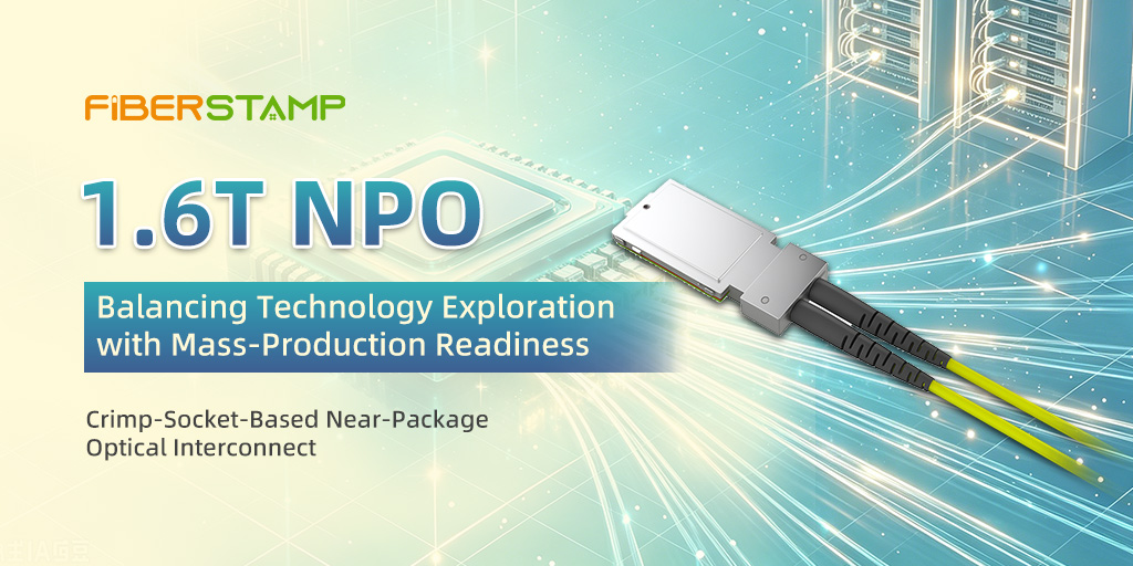
Singapore, September 29, 2026 — As AI computing continues to scale rapidly, 1.6T near-package optical interconnect technology is approaching a critical transition from sample validation to commercial deployment. FIBERSTAMP has completed a shippable engineering sample of a socket-based 1.6T NPO solution defined under OIF standards, demonstrating the transmission performance of near-package optical interconnects for ultra-high-bandwidth applications.
However, thermal expansion mismatch associated with flip-chip processes, together with the challenge of maintaining consistent socket compression at high-volume production scale, presents significant barriers to mass production. These challenges remain important factors limiting the large-scale deployment of NPO technology in million-unit-class data center environments.
Material Constraints Associated with Flip-Chip Bonding
Different packaging materials have different coefficients of thermal expansion. During long-term high- and low-temperature cycling in data centers, combined with continuous high-power operation, microscopic mechanical stress can accumulate and shift over time, directly affecting optical coupling loss.
Maintaining consistent performance across production batches remains challenging, while meeting long-term reliability requirements under the stringent lifecycle qualification standards of cloud service providers can be difficult. These factors can significantly increase the cost of yield management and quality control during mass production.
Socket Press-Fit Assembly Consistency
NPO relies on socket-based press-fit assembly to achieve high-density interconnection. During high-volume manufacturing and field installation, even small variations in press-fit force or alignment tolerances can result in unpredictable differences in optical performance.
For data center clusters deployed at million-unit scale, uncontrolled assembly variation can directly translate into higher operation and maintenance costs, creating significant risks for large-scale commercial procurement.
A Disciplined Approach to Technology Evaluation
FIBERSTAMP’s investment in socket-based 1.6T NPO reflects a comprehensive and disciplined approach to technology evaluation. The company validates emerging architectures early to maintain its ability to explore next-generation computing interconnects, while maintaining a rational assessment of their commercial viability.
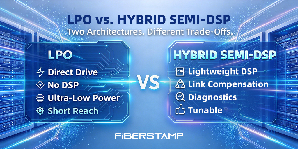
FIBERSTAMP clearly distinguishes between technical feasibility in the laboratory and manufacturability at data center scale. Rather than committing to a single technology path, the company pursues multiple architectures in parallel, accumulating engineering data and developing a deeper understanding of the benefits, limitations, and trade-offs associated with each approach.
The competition in high-speed optical interconnects has never been simply a race to produce a prototype first. It is a full-lifecycle test spanning R&D, manufacturing, delivery, deployment, and long-term operation and maintenance.
From trial validation of press-fit socket-based 1.6T NPO near-package optical interconnects to preparations for CPX-standardized solutions for the 224G era, FIBERSTAMP remains focused on real-world customer deployment requirements. By balancing performance, power consumption, reliability, and mass-production costs, FIBERSTAMP is committed to providing global AI computing clusters with high-speed interconnect solutions that are practical, scalable, and ready for large-scale deployment.
Exploring Technology While Advancing Commercialization with Discipline
As computing infrastructure undergoes rapid transformation, FIBERSTAMP continues to pursue a multi-path technology strategy, working alongside customers to navigate the next generation of high-speed optical interconnect technologies and their ongoing evolution.