Silicon photonics originated in 1985 when Professor Soref first proposed the concept of using silicon as the optical waveguide medium. This innovative principle was visionary at the time because silicon is an abundant and cost-effective material, and it had already found widespread applications in the field of electronics.
Over 40 years, silicon photonics has made significant advancements. It has transitioned from initial laboratory research to becoming an engineering product widely applied in fields such as communication and sensing. Whether it’s the performance of individual components, including improvements in modulator and detector bandwidths, continuous optimization of passive devices, or the scale of systems, progressing from small systems consisting of a few components to large-scale silicon photonic chips comprising thousands or even tens of thousands of optical devices, the number of devices has entered the realm of Very-Large-Scale Integration (VLSI).
Technical Principles and Development of Silicon Photonics
The technical principles of silicon photonics are based on the optical properties of silicon material. Silicon serves as an excellent optical waveguide medium, allowing for effective control of optical signals.
SiN waveguides and their advantages: Currently, most silicon photonics fabs offer single-layer or double-layer SiN waveguides. SiN waveguides are highly regarded due to their larger size and higher tolerance for waveguide fabrication errors. These waveguides are well-suited for designing phase-sensitive passive components like Mux/DeMux. Furthermore, SiN waveguides exhibit low transmission losses, making them particularly suitable for optical waveguide routing within larger-sized photonic chips. Due to the refractive index of SiN falling between silicon and SiO2, its confinement ability is relatively weaker, resulting in SiN-based edge couplers having larger mode field sizes and lower coupling losses when interfacing with single-mode optical fibers.
Fundamental Principles of Silicon Photonics Modulators: Currently, silicon photonics modulators primarily operate based on the plasma dispersion effect. This means that by altering carrier concentration, the refractive index of silicon waveguides can be changed. This change induces variations in optical intensity through optical interference structures, effectively embedding electrical signals into optical signals. However, the plasma dispersion effect is relatively weak, necessitating higher driving voltages for optical signal modulation.
Introduction of New Materials: To enhance the performance of silicon photonics modulators, researchers have been actively working on introducing new materials. These include GeSi-based EAM modulators, and although they exhibit higher insertion losses, some silicon photonics foundries are involved in related device development. One approach involves designing quantum well structures to extend the operating wavelength into the O-band. Additionally, the introduction of III-V materials onto the silicon platform, as undertaken by Intel in process development, is a viable path. III-V materials can be employed not only in manufacturing lasers and SOAs but also as modulators. Another potential solution is using materials like lithium niobate (LiNbO3), BTO, and others, which rely on the Pockels effect for electro-optic modulation and offer extremely high intrinsic bandwidth. This could be a critical technology choice for increasing the speed of high-speed optical communication.
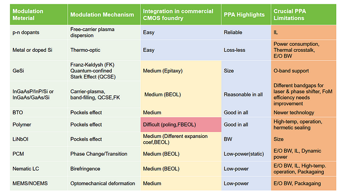
Challenges and Prospects: While the introduction of new materials provides more performance possibilities for silicon photonics modulators, it also comes with process challenges. For instance, integrating III-V materials that are not compatible with CMOS processes into silicon photonics fabs and performing micro-nano structure processing remains an unresolved issue. Additionally, low-power modulation technologies like PCM (phase-change material) and MEMS are suitable for scenarios with strict power consumption requirements. Overall, the electro-optic modulation effect of silicon material is relatively weak, but through the introduction of novel materials, these challenges may be overcome in the future to meet the demands of high-speed optical communication. Key criteria for evaluating these technologies include PPA (power, performance, area) and HVM (high-volume manufacturing), and silicon photonics modulators of the future may make significant breakthroughs in these aspects.
Future Trends and Prospects of Silicon Optical Technology
When it comes to laser integration in silicon photonics technology, there are several feasible approaches. Here is a brief overview of these six schemes:
a. Traditional FSO (Free Space Optics) Approach: This method employs an external laser source to guide laser light onto the silicon chip through optical components like lenses and isolators. It’s a conventional approach but involves complex optical elements, which may increase system costs.
b. In-chip Device Optimization: By optimizing the components within the optical chip to reduce reflections and minimize light signal loss. This can reduce the number of external components in the system, lowering costs.
c. Photonic Wire Bonding: Using photonic wire bonding technology to process a three-dimensional polymer waveguide between the laser chip and the silicon photonics chip for light signal transmission. This can reduce coupling losses and enhance efficiency.
d. Flip-Chip and Transfer Print: This method involves flipping (Flip-Chip) or transfer printing (Transfer Print) the laser chip onto the silicon photonics chip and then coupling the light signal into the silicon photonics chip using edge coupling. This helps reduce device size and improve performance.
e. III-V Material Heterogeneous Integration: Introducing III-V materials onto the silicon photonics chip and then forming lasers through processes like etching. This approach may require overcoming challenges related to CMOS process compatibility and micro/nanostructure fabrication.
f. Silicon-based Epitaxial Growth of Quantum Dot Lasers: This is a more long-term solution in which III-V materials are directly epitaxially grown on silicon to create quantum dot lasers. While it holds promise, many technical challenges need to be addressed.
Considering the evolving demands of the future, it’s evident that multi-wavelength light sources will play a significant role, bringing numerous advantages. Particularly, optical comb light sources have garnered significant attention. Optical combs, while potentially lagging behind traditional DFB laser arrays in terms of output power and signal-to-noise ratio, offer smaller dimensions and hold tremendous potential in high-bandwidth and large-scale silicon photonics chips.
The prospects for optical comb technology are highly appealing, even though there are still some unresolved technical issues. However, it may become a critical component of silicon photonics technology in the future, further driving innovation and development in fields like optical communication and sensing. The ongoing advancements in this field will provide us with more choices to meet the ever-growing communication demands.