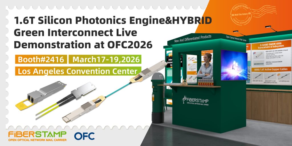
Singapore, March 12, 2026 — As global data center networks rapidly accelerate toward the 800G and 1.6T era, ultra-high-speed optical interconnect technologies are entering a new phase of innovation. OFC 2026, held at the Los Angeles Convention Center, brings together leading innovators across the optical communications industry. At this year’s exhibition, FIBERSTAMP showcases its next-generation technologies for AI-driven and hyperscale data center networks, featuring the 1.6T NPO silicon photonics engine and the HYBRID green interconnect architecture. These innovations introduce a new technological pathway for upgrading ultra-high-speed optical interconnects.
FIBERSTAMP Booth: #2416
Live Demonstration of the 1.6T DR16-NPO Silicon Photonics Engine
The 1600G NPO DR16 silicon photonics engine, built on linear direct-drive technology, represents one of FIBERSTAMP’s key innovations for the next generation of optical networking.
The solution adopts a linear silicon photonics engine architecture, utilizing a socket-based packaging design combined with LPO linear direct-drive technology and advanced flip-chip bonding processes.
Compared with conventional NPO/CPO architectures, the linear NPO silicon photonics engine eliminates the DSP, significantly reducing system-level power consumption and overall cost.
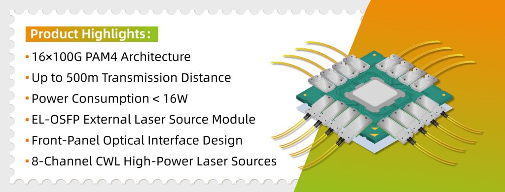
Key Performance Specifications
Transmitter
The transmitter demonstrates excellent optical eye performance with a typical TDECQ of only 2.2 dB. The solution is fully compliant with the IEEE 802.3bs DR4 standard and enables seamless interoperability with conventional DSP-based DR4 optical modules, supporting hybrid deployment between new and legacy architectures.
Receiver
At a BER of 1E-6, the receiver sensitivity across all channels is better than −5 dBm, ensuring sufficient link budget for stable high-speed transmission.
Launch of HYBRID Green Interconnect Innovations at OFC 2026

The 800G OSFP HYBRID product family differs from traditional full-DSP optical modules (DPO). By utilizing DSP processing on only half of the channels, the HYBRID architecture significantly improves both power efficiency and latency performance.
HYBRID optical modules and active optical cables draw inspiration from general design methodologies used in LPO and LRO architectures. From the perspective of strict system-level signal alignment, however, HYBRID introduces a more advanced design strategy that balances performance, power consumption, and deployment flexibility.
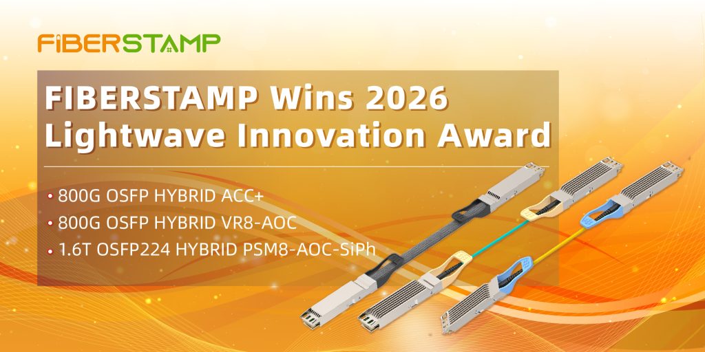
HYBRID Green Interconnect Products Demonstrated at OFC 2026
- 800G OSFP HYBRID VR8-AOC — Live demonstration
- 800G OSFP-PHO 2×DR4 — Live demonstration
- 800G OSFP HYBRID PSM8-AOC
FIBERSTAMP HYBRID Architecture Patent Overview
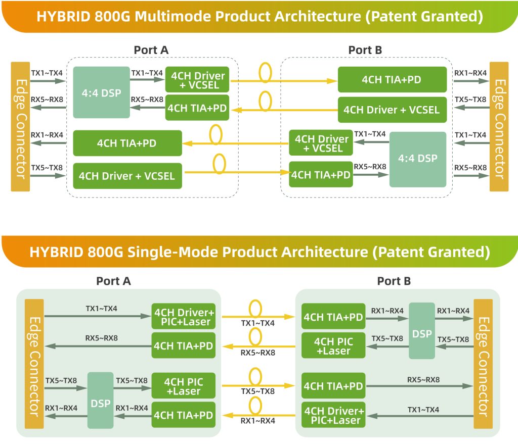
HYBRID Architecture: Advantages and Key Considerations
1. Key Advantages of HYBRID
Significant Power Reduction:
Approximately 20–30% lower power consumption compared with full-DSP solutions
Ultra-low Link Latency:
With only half the DSP processing, latency is reduced by approximately 50%, approaching performance levels similar to LRO architectures.
Reliable Signal Quality:
- Multimode 50 m: PRE-FEC BER E-7 / E-8
- Single-mode 500 m: PRE-FEC BER E-10
Optimized Cost Structure:
Overall system cost can be reduced by approximately 20% compared with traditional DSP-based architectures.
Higher Channel Density Capability:
Provides a feasible architecture for 16-channel / future 3.2T pluggable optical modules.
2. Limitations and Engineering Considerations
Non-DSP receiver channels require slightly tighter host-side SI tuning.
System-level co-optimization is required rather than simple plug-and-play deployment
Large-scale commercialization is still in its early stage and requires close collaboration with ecosystem partners.
Nevertheless, compared with LPO and LRO architectures, the engineering risks associated with the HYBRID architecture are significantly more manageable.
Advancing Next-Generation Optical Interconnects
The HYBRID architecture achieves a balanced optimization across power consumption, latency, cost, and performance, making it a promising technology pathway for next-generation high-speed optical interconnects.
As demand for AI infrastructure and hyperscale computing networks continues to grow, FIBERSTAMP will continue advancing silicon photonics technologies, linear-drive architectures, and green interconnect solutions. The company looks forward to working closely with switch vendors, system providers, and end users to accelerate the large-scale deployment of 800G and 1.6T optical interconnect technologies, enabling scalable and energy-efficient next-generation data center networks.