In the domain of commercial silicon photonics integration, there exists a clear division into two factions: the III-V family and silicon (Si). The III-V family technology, while mature, is burdened by high costs and incompatibility with CMOS (Integrated Circuit) technology. Conversely, Si silicon devices, leveraging CMOS technology, facilitate passive optoelectronic device integration and single-chip integration, enabling extensive scalability and boasting remarkable density.
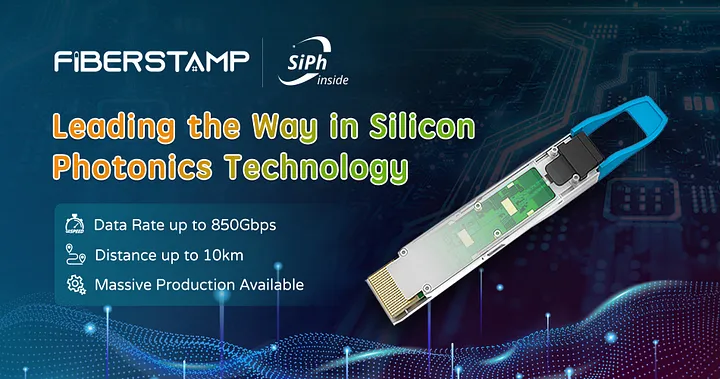
Significantly, silicon photonics chips are harmonious with CMOS technology, showcasing superior speed, bandwidth, and performance in comparison to III-V family optical devices. Consequently, in the production of devices surpassing 400G, 800G, and 1.6T rates, the manufacturing processes and device performance display exceptional capabilities. Now, let’s delve into a cost-effective architecture solution for 400G rate data center architecture, integrating 4-channel optics, silicon photonics, and 100G PAM4 technology provided by FIBERSTAMP.
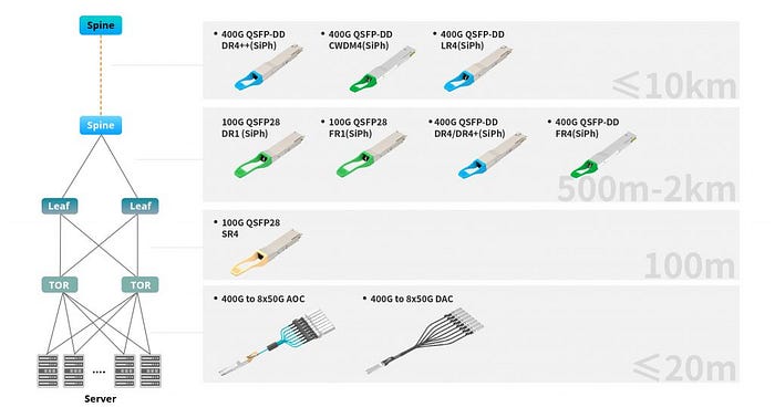
The combination of 4x100G PAM4 electrical interface and 400G QSFP112 SR4 and DR4 silicon photonics technology achieves high integration with fewer connections, resulting in reduced power consumption and cost savings. This product line includes the following silicon photonics optical modules: 400G QSFP112 DR4/DR4+, 400G QSFP112 FR4, 400G QSFP112 CWDM4/LR4.
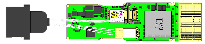
The core technology within FIBERSTAMP’s silicon photonics modules revolves around innovative free-space COB high-coupling efficiency packaging design and MZI software locking algorithms. In terms of silicon photonics cores, collaborative efforts with partners have yielded joint designs for multiple silicon photonics chips.
Advantages of silicon photonics include high production yield, cost efficiency, compact spatial utilization, polarization splitting and rotation, superior signal quality over EML, and temperature-insensitive modulators. Additionally, it delivers high output optical power and longer transmission distances compared to EML. However, it’s pivotal to note that silicon photonics modules lack native lasers and grapple with limitations in lossy modulators.
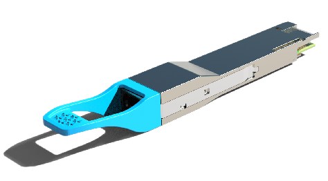
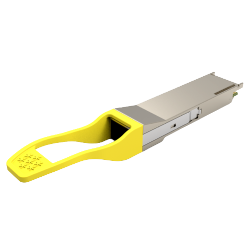
Now, let’s closely examine FIBERSTAMP’s 400G DR4/DR4+/DR4++ Silicon Photonics Optical Modules Series.
400G QSFP-DD DR4/DR4+/DR4++ Features with
QSFP-DD MSA and CMIS compliant
Compliant to 802.3cu
8×53.125Gbit/s PAM4 electrical interface(400GAUI-8)
4×106.25Gbps(53.125GBd PAM4)Optics architecture
Power consumption <10W
Maximum link length of 500m/2km/10km G.652 SMF with KP4-FEC
MPO-12 receptacles
Built-in digital diagnostic functions
Operating case temperature 0°C to +70°C
3.3V power supply voltage
RoHS compliant(lead free)
400G QSFP112 DR4/DR4+/DR4++ Features with
- QSFP112 MSA and CMIS compliant
- Compliant to 802.3cu
- 4×106.25Gbps PAM4 electrical interface
- 4×106.25Gbps PAM4 Optics architecture
- Power consumption <10W
- Maximum link length of 500m/2km/10km G.652 SMF with KP4-FEC
- MPO-12 receptacles
- Built-in digital diagnostic functions
- Operating case temperature 0°C to +70°C
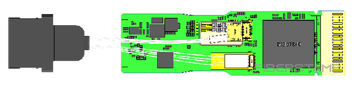
The transmitter utilizes a highly integrated silicon photonics solution, while the receiver employs a PIN detector. OMA RX sensitivity meets -7.1dBm @ 2.4E-4 Pre-FEC 53.125GBd, consuming less than 10W of power.
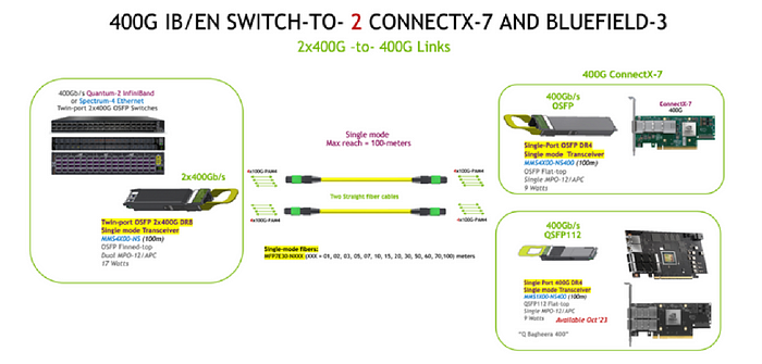
NVIDIA’s application: 400G IB/EN Switch — 2 CONNECTX-7 and BLUEFIELD-2x400G to 400G link.
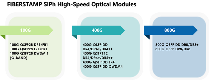
FIBERSTAMP provide a differentiated product line of high-speed silicon photonics modules, as follows
With the maturation of silicon photonics technology, cost-effective 400G data centers are approaching maturity and commercialization. The integration of silicon photonics technology enables more efficient data processing, transmission, and reception. Reduced signal loss, component integration, and optimized power usage collectively contribute to enhancing energy efficiency and cost-effectiveness in data centers.