1. Building Low-Latency and Low-Power Data Center Interconnect Networks with NRZ Modulation and Half-DSP Technologies
Within AI computing data center networks, NRZ (Non-Return-to-Zero) modulation and “Half-DSP” / linear-drive solutions, including LPO (Linear Pluggable Optics) and Hybrid architectures, have become important technology approaches for achieving both low latency and low power consumption.
These two technology paths are designed for different data rates and transmission distance scenarios. The core objective is to meet the requirements of high-speed interconnects while addressing the high power consumption and latency challenges associated with traditional full-DSP optical modules.
1.1 NRZ Modulation: Mature, Reliable, and Optimized for Ultra-Low Latency
NRZ is a traditional binary modulation technology where each symbol carries one bit of information. In short-distance interconnect applications, its simple physical-layer characteristics make it a preferred solution for latency-sensitive networks.
Application Scenarios
NRZ is mainly used in interconnect scenarios with single-channel speeds ≤200Gbps.
With continued technology evolution, some high-performance SerDes solutions are exploring NRZ-based optimization approaches for higher-speed applications. However, mainstream high-speed optical interconnects at 400G/800G and beyond have transitioned to PAM4 modulation.
Key Advantages
Ultra-Low Latency
NRZ does not require complex digital signal processing (DSP) for signal equalization and error correction. The electrical-to-optical conversion process introduces almost no additional processing latency.
Low Power Consumption
With a simpler circuit architecture and without the high power overhead of DSP chips, NRZ-based optical modules typically maintain low power consumption levels, generally within several watts.
High Signal-to-Noise Ratio Tolerance
In optical fiber transmission, channel loss is relatively low. The two-level NRZ signal provides strong resistance to interference and maintains good signal integrity.
Limitations
NRZ has relatively low spectral efficiency and cannot efficiently support high-speed transmission beyond 50Gbps per wavelength.
Therefore, in mainstream 400G/800G and higher-speed data center and AI computing interconnect architectures, NRZ is gradually being replaced by PAM4 modulation.
FIBERSTAMP’s 200G QSFP-DD S8/PSM8 parallel optical module represents a milestone product in this field.
1.2 “Half-DSP” Modulation Solutions: LPO and Hybrid Technologies
“Half-DSP” is not a formal industry standard term. It generally refers to reduced-DSP or DSP-free optical architectures, including:
LPO (Linear Pluggable Optics)
Hybrid / LRO (Linear Receive Only)
These solutions aim to maintain sufficient signal integrity while significantly reducing the power consumption and latency associated with traditional full-DSP optical modules.
LPO (Linear Pluggable Optics)
The LPO architecture completely removes the DSP chip from the optical module and retains only the linear driver and TIA (Transimpedance Amplifier).Signal processing and equalization are mainly handled by the advanced equalization capability of the switch-side ASIC.
Hybrid (Half Retimed & Half Linear) / LRO (Linear Receive Only)
Hybrid solutions typically retain partial linear-drive functionality at the transmitter or receiver side, or utilize simplified DSP logic in specific signal paths to achieve a balance between performance and power efficiency.
Key Characteristics
Balanced Power Efficiency and Performance
Compared with LPO, Hybrid solutions can provide improved signal integrity for longer transmission distances (such as 100m–2km) while still achieving approximately 20%–30% power savings compared with full-DSP solutions.
Latency Optimization
Although some signal processing capability is retained, simplified algorithms or reduced DSP functions enable significant latency reduction.
Application Scenarios
Hybrid and LRO solutions are suitable for 100m–2km short-to-medium distance interconnect applications, where transmission distance requirements remain important while power efficiency is highly valued.
Core Technology Comparison
| Solution Type | Technical Principle | Latency Performance | Power Advantage |
| LPO (Linear Pluggable Optics) | Completely removes the DSP chip and uses linear drivers to directly drive optical components | Ultra-low latency (no DSP processing delay) | Highest power efficiency (significant power reduction) |
| Hybrid / LRO | Retains partial DSP functionality or simplified DSP algorithms combined with linear-drive technology | Ultra-low latency (DSP functions reduced, processing latency significantly reduced) | Significant reduction compared with full DSP |
| Full DSP | Uses complete DSP processing for complex equalization and error correction | Higher latency due to digital processing | Higher power consumption (DSP accounts for a significant portion of module power) |
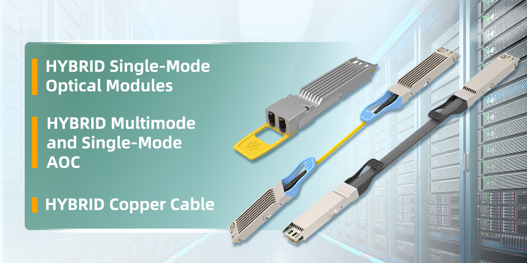
FIBERSTAMP’s Half-DSP / Hybrid optical modules and active optical cable (AOC) product portfolio represent engineering innovations in this field, providing practical solutions for large-scale network deployment with enhanced feasibility compared with traditional LPO/LRO approaches.
Representative products include:
HYBRID Single-Mode Optical Modules
| Product Type | Wavelength | Laser Source (LD) | Optical Detector (PD) | Maximum Transmission Distance / Length | Optical Interface | Maximum Power |
| 800G OSFP-HRO 2×DR4 Optical Module | 1310nm | SiPh | PIN | 500m | Dual MPO | 13W |
| 1.6T OSFP224-HRO 2×DR4 Optical Module | 1310nm | SiPh PIN | PIN | 500m | Dual MPO | 21W |
HYBRID Multimode and Single-Mode AOC
| Product Type | Wavelength | Laser Source (LD) | Optical Detector (PD) | Maximum Transmission Distance / Length | Optical Interface | Maximum Power |
| 400G QSFP-DD HYBRID VR8 Active Optical Cable | 850nm | VCSEL | PIN | 50m | AOC | 6.6W |
| 800G OSFP HYBRID VR8 Active Optical Cable | 850nm | VCSEL | PIN | 50m | AOC | 9W |
| 800G OSFP HYBRID PSM8 Active Optical Cable | 1310nm | Silicon Photonics (SiPh) | PIN | 500m | AOC | 12.5W |
| 1.6T OSFP224 HYBRID PSM8 Active Optical Cable | 1310nm | Silicon Photonics (SiPh) | PIN | 500m | AOC | 21W |
HYBRID Copper Cable Solutions
| Product Type | Laser Source (LD) | Optical Detector (PD) | Maximum Transmission Distance / Length | Optical Interface | Maximum Power |
| 800G OSFP HYBRID Enhanced Active Copper Cable (ACC+) | N/A | N/A | 6m+ | N/A | 7W |
| 1.6T OSFP224 HYBRID Enhanced Active Copper Cable (ACC+) | N/A | N/A | 4m | N/A | 13W |
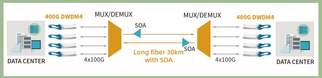
2. O-BAND Non-Coherent DWDM as an Efficient Complement to Coherent Communication for Low-Latency and Cost-Effective Medium-Distance DCI
With the rapid growth of AI computing clusters and distributed data centers, Data Center Interconnect (DCI) networks are facing increasing demands for 400G/800G/1.6T high-speed optical interconnect solutions.
Although traditional coherent communication technologies provide excellent long-distance transmission capabilities, their complex DSP architecture, high power consumption, higher cost, and increased transmission latency have created efficiency and cost challenges for short- and medium-distance DCI applications within 30km.
To address this challenge, FIBERSTAMP has introduced an O-BAND (1310nm window) non-coherent DWDM product portfolio.
By leveraging the natural zero-dispersion characteristics of the O-BAND window, this architecture eliminates the need for DCM (Dispersion Compensation Module) and enables an efficient transmission solution optimized for medium-distance data center interconnect applications.
Compared with traditional C-BAND coherent solutions, O-BAND non-coherent DWDM provides the following key advantages:
Low Latency: By eliminating complex DSP-based dispersion compensation processing, the solution significantly reduces link transmission latency, making it highly suitable for latency-sensitive applications such as AI training and Real-time computing resource scheduling .
Low Power Consumption: By adopting Silicon Photonics integration technology and PAM4 modulation architecture, the overall power consumption is significantly lower than traditional coherent optical modules.
Cost Efficiency: The architecture eliminates the need for expensive coherent components, DCM modules, and complex optical line system designs, significantly reducing: CAPEX, Network deployment cost and Operation and maintenance expenses.
High-Density Deployment: The solution supports high-density optical module form factors including QSFP-DD and OSFP,meeting the requirements of next-generation large-scale data center deployments.
Open and Flexible Architecture: The solution supports open optical networking architectures and is compatible with white-box switches , open optical line systems and Improving overall network flexibility and deployment efficiency.
From 100G to 800G and further toward 1.6T, FIBERSTAMP has established one of the industry’s most complete O-BAND DWDM pluggable product portfolios, covering different generations and capacity requirements for data center interconnect networks.
Product Portfolio:
1. 100G QSFP28 DWDM1
- Single wavelength 100G transmission
- Simplified deployment and operation
- System supports up to 16-channel wavelength transmission
2. 200G/400G QSFP-DD DWDM4
- 4-wavelength aggregation
- 50G/100G per wavelength
- System supports up to 16-channel wavelength transmission
3. 800G OSFP/QSFP-DD 2×PSM DWDM4 (O-BAND)
- Single wavelength 100G PAM4
- System supports up to 16-channel wavelength transmission
4. 1.6T OSFP224-EL 2×PSM DWDM4 (O-BAND)
- Single wavelength 200G PAM4
- External light source architecture
- System supports up to 16-channel wavelength transmission
O-BAND DCI Interconnect Application Scenario
Transmission Distance: 2km–30km
3.Three Flexible Solutions for 1.6T AI & Data Center Interconnect
With the explosive growth of AI computing requirements, data center interconnect bandwidth is rapidly evolving from 400G/800G toward 1.6T.
To meet deployment requirements across different application scenarios, the industry is developing three major technology approaches for 1.6T optical interconnects. Each solution provides different advantages and is optimized for different requirements in terms of cost structure ,power budget and deployment scalability.
3.1 Standard 1.6T Pluggable Optical Transceiver
Standard 1.6T OSFP224 Optical Module
The 1.6T OSFP224 optical module is a next-generation high-speed optical transceiver featuring:
- Total bandwidth of 1.6Tbps
- OSFP224 form factor
- Designed to support AI clusters and high-performance computing bandwidth requirements
It represents one of the mainstream solutions for next-generation AI networking deployments.
Core Parameters and Definition
Data Rate and Form Factor
Total Data Rate: 1.6Tbps total bandwidth is achieved through 8 × 200G PAM4 electrical channels
After protocol overhead, the effective payload reaches approximately 1.6Tbps.
OSFP224 Form Factor
OSFP224 is an evolution of the traditional OSFP form factor. It features:
- 224 electrical contacts
- Support for 16 electrical lanes
- Higher port density
- Enhanced thermal capability
It is designed for high-density AI switch deployments.
Standard 1.6T Pluggable Module Solutions
| Product Type | Transmission Architecture | Transmission Distance | Key Advantages | Application Scenario |
| 1600G OSFP DR8 | 8 parallel single-mode fibers, each lane 200G | 500m | Mature solution, optimized for short-distance interconnect | AI cluster rack-to-rack / intra-row interconnect |
| 1600G OSFP 2×FR4 | Two FR4 channels, each using 4 wavelength WDM | Approx. 2km | Saves approximately 75% fiber resources and improves cabling flexibility | Longer-distance data center interconnect |
3.2 External Light Source 1.6T Pluggable Optical Module (ELS-Pluggable)
This architecture separates the laser source from the 1.6T OSFP224 optical module.
A centralized:
- Rack-level external light source
- Board-level external light source
- Co-packaged light source
provides optical power to multiple pluggable modules through fiber coupling.
The optical module itself only retains modulators and photodetectors and required electrical processing components. This architecture significantly reduces thermal load at the individual module level.
As one of the pioneers proposing the External Light Source 1.6T Pluggable Optical Module architecture, FIBERSTAMP provides the following solutions:
| Product Type | Transmission Architecture | Transmission Distance | Key Advantages | Application Scenario |
| 1600G OSFP DR8 EL | 8 parallel single-mode fibers, each lane 200G | 500m | External light source significantly reduces optical module power consumption | AI cluster rack-to-rack / intra-row interconnect |
| 1600G OSFP 2×FR4 EL | Two FR4 channels, each using 4 wavelength WDM | Approx. 2km | External light source significantly reduces optical module power consumption | Longer-distance data center interconnect |
3.3 External Light Source 1.6T (16×100G) NPO Solution
Near-Package Optics (NPO)
The NPO architecture represents a transition technology between pluggable optics and Co-Packaged Optics (CPO). In the NPO architecture, the optical engine is no longer integrated inside the switch ASIC package.
Instead, it is installed immediately outside the package:
Optical engine distance from ASIC: <50mm
Combined with an external light source, NPO enables ultra-short-distance high-speed interconnects through:
Silicon Photonics
Polymer waveguide technologies
The 1.6T NPO solution is typically deeply integrated with Silicon Photonics platforms to achieve extremely low electrical-to-optical transmission loss.
It should be noted that practical NPO optical engine architectures generally need to be based on:
16×100G physical architecture
32×100G physical architecture
This represents the key differentiation point compared with 1.6T pluggable optical modules.
Although the industry is exploring:
- 3.2T NPO
- 6.4T NPO
Architectures based on 224G SerDes technology, related standards have not yet been finalized.
Comparison of Three 1.6T Solutions
| Comparison Dimension | Standard 1.6T Pluggable Module | External Light Source 1.6T Pluggable Module | External Light Source 1.6T NPO Solution |
| Light Source Location | Integrated inside module | Rack-level / board-level external | Rack-level / board-level external |
| Optical Engine Location | Inside module | Inside module | Outside ASIC package |
| Power Efficiency (pJ/bit) | Higher | Medium | Lowest (best efficiency) |
| Port Density | Medium | Medium | High |
| Compatibility with Existing Infrastructure | High (plug-and-play) | High | Low (requires motherboard/rack redesign) |
| Maintenance and Replacement | Best | Good | Complex (requires specialized operation) |
| Thermal Management | High (module self-heating) | Medium (centralized light source management) | Low (heat separation and high efficiency) |
| Transmission Distance | Medium/short distance (≤2km) | Medium/short distance (≤2km) | 500m-2km |
| System Architecture Complexity | Low | Medium | High |
| Standardization Maturity | Mature (defined by OIF/IEEE) | Under development | Mature & OIF-standard supported |
Deployment Roadmap
The three solutions are not mutually exclusive alternatives.
Instead, they represent a layered deployment strategy targeting different technology maturity stages and application scenarios.
Near Term (2024–2026): Standard pluggable optical modules will remain the mainstream solution, supporting smooth upgrades for most data center deployments.
Mid Term (2027+): External light source pluggable architectures are expected to achieve rapid adoption in large-scale AI clusters by balancing deployment flexibility and power optimization
Long Term (2027+): With the maturity of Silicon Photonics technology and standardization progress, NPO solutions are expected to become a major architecture for AI supercomputing interconnects, providing the foundation for future 3.2T and 6.4T network evolution.
4.Enabling Ultra-Low Latency All-Optical Switching at Critical Network Nodes with AWGR + EDFA / AWGR + SOA Architectures
4.1 AWGR (Arrayed Waveguide Grating Router)
AWGR is a passive wavelength routing engine that utilizes its cyclic wavelength routing characteristics to deterministically map different optical wavelengths within a WDM signal to corresponding output ports.
Unlike traditional electrical switching architectures, AWGR does not require lookup tables, packet scheduling and optical buffering.
Therefore, it completely eliminates the traditional optical-electrical-optical (O-E-O) conversion process in electrical switching systems.
The optical signal remains entirely in the optical domain throughout the transmission process.
A single-stage optical switching operation introduces only nanosecond-level latency, which is:
- 2–3 orders of magnitude lower than traditional OEO architectures
- Highly deterministic with extremely low latency jitter
This capability makes AWGR-based optical switching highly suitable for:
- AI computing clusters
- Low-latency computing networks
- High-performance computing scheduling applications
4.2 AI Computing Cluster AWGR + EDFA Optical Switching Topology
1. Architecture Overview
This architecture is mainly designed for data center inter-rack optical switching and cross-campus long-distance all-optical switching hubs.The topology adopts a three-level flattened architecture:
Compute Access Layer → Core Wavelength Switching Layer → Optical Amplification Output Layer
Access Layer
- Each AI computing node / GPU server outputs optical signals through:
- 100G PSM DWDM4 (C-BAND) optical modules
- Each optical port directly carries:
- Four fixed C-band wavelengths
- The optical signals are then aggregated through a:
- DWDM multiplexer (MUX)
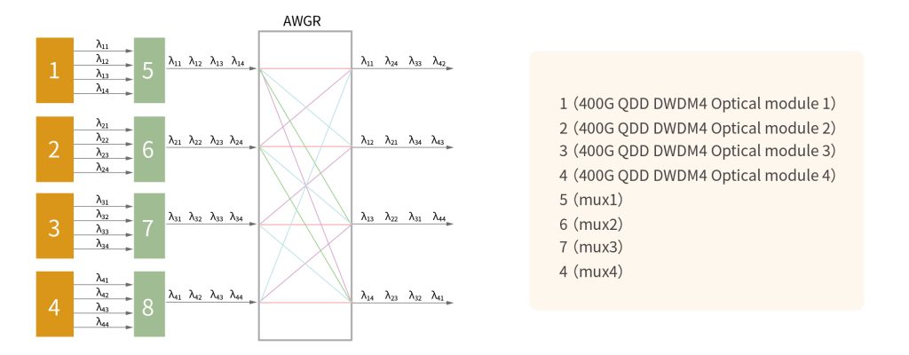
Core Switching Layer
- After wavelength multiplexing, signals are transmitted into an:
- N×N AWGR wavelength router
- The AWGR performs optical routing switching based on wavelength assignment.
- The switching process is completed entirely in the optical domain.
Optical Compensation Output Layer
- After AWGR switching, the system experiences approximately:
- 8dB inherent insertion loss
- An EDFA (Erbium-Doped Fiber Amplifier) is used to compensate for this optical loss.
- The amplified signal is then transmitted to:
- Next-stage switching nodes
- Target computing clusters
- Supporting transmission distances at the:
- 10km level
2. Topology Characteristics
Key advantages include:
- No multi-stage O-E-O conversion
- Core switching latency below 1μs
- Simplified network architecture
- Suitable for large-scale computing hubs with relatively stable network topology
Technical Parameter Comparison
| Parameter | Traditional Electrical Switching (OEO) | AWGR + EDFA All-Optical Switching |
| Switching Latency | 500ns ~ several μs | <10ns (single stage) |
| Latency Jitter | Several μs ~ ms (queue variation) | <1ps (after thermal control) |
| O-E-O Conversion | 1–2 conversions per port | 0 (fully optical domain) |
| Single Port Power Consumption | 15–25W / 100G | 0.1–0.5W / 100G (EDFA shared) |
| 1000-Port Power Consumption | 15–25kW | ~455W (80-channel example) |
| Protocol Dependency | Requires IP/MPLS header processing | Fully transparent, protocol independent |
| Buffer Queuing | Exists, introduces unpredictable latency | None, wavelength-based routing |
| Signal Format Transparency | Not transparent, format dependent | Transparent (OOK/QPSK/QAM) |
3. AI Computing Cluster AWGR + SOA Optical Switching Topology
This architecture is mainly designed for:
- In-rack optical switching
- Same data center high-density optical switching hubs
- Ultra-low latency AI cluster interconnects
The topology adopts a compact architecture combining:Active Scheduling + All-Optical Switching + Integrated Optical Amplification
Wavelength Scheduling Layer
Each computing node connects to:
- O-BAND DWDM optical components
- O-BAND multi-wavelength tunable optical engines
The scheduling controller dynamically adjusts output wavelengths according to GPU communication requirements, including Gradient synchronization and Parameter broadcasting.
FIBERSTAMP provides O-BAND DWDM parallel optical modules with different baud rates to support medium-distance AI computing interconnect applications.
Core Optical Switching Layer
The dynamically scheduled wavelength signals are transmitted into:
AWGR wavelength routers
The AWGR performs:
- Wavelength-based optical routing
- Nanosecond-level optical path switching
Integrated Optical Amplification Layer
The architecture uses:
SOA (Semiconductor Optical Amplifier)
for amplification of weak optical signals after switching.
Compared with EDFA, SOA provides:
- Smaller form factor
- Better integration capability
- Suitability for high-density rack deployment
SOA can also assist with:
- Wavelength conversion
- Enhanced scheduling flexibility
Topology Characteristics
The complete switching process latency can be reduced to:
- Below 100 nanoseconds
- The power consumption of a single optical switching chip is approximately:
- 1/10 of a comparable electrical switching ASIC
This architecture is highly suitable for:
- Large-scale AI training clusters
- Thousands of GPU interconnect environments
- Low-latency east-west GPU communication
The network architecture diagram
Key Node Selection Recommendations
| Dimension | AWGR + EDFA | AWGR + SOA |
| Application Scenario | Backbone network core hubs, large-scale intelligent computing centers, long-distance rack interconnect | Data center internal networks, high-frequency trading, AI cluster short-distance low-latency interconnect |
| Switching Granularity | Wavelength-level (coarse granularity), microsecond-level switching | Wavelength/time-slot level (fine granularity), sub-nanosecond switching |
| Latency Performance | Fixed physical latency + microsecond-level reconfiguration overhead | Fixed physical latency + sub-nanosecond reconfiguration overhead |
| Signal Quality | High (low noise, suitable for long-distance transmission) | Medium (requires consideration of nonlinear effects and noise accumulation) |
